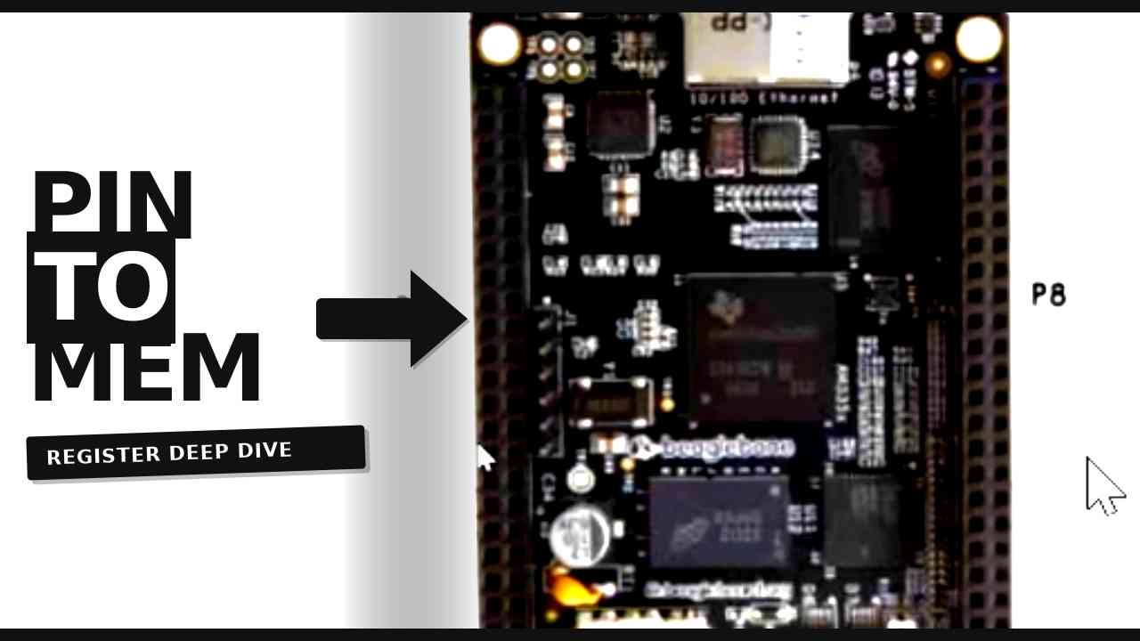
Why I Built This Table
A few posts back I walked through resolving a single header pin
(P9_12) to its gpiochip/line number with gpioinfo. That workflow is great when you
already know which pin you're chasing. What it doesn't give you is the bird's-eye view — every pin on
both 46-pin headers, in one place, so you can pick a free GPIO for a project without flipping between
the datasheet, the System Reference Manual, and a terminal. This post is that bird's-eye view.
How to Read This Table
- Header/Pin — the silkscreen label printed on the board (e.g.
P9_12). - GPIO Bank_Offset — the AM335x GPIO bank (0–3) and offset within that bank (0–31), e.g.
GPIO1_28. - Linux GPIO # — the flattened number the classic sysfs interface (
/sys/class/gpio) and most tutorials use, computed asbank × 32 + offset. - Default Function — the pin's most commonly-used alternate (non-GPIO) mux mode on the stock device tree, if it has one.
One caveat worth repeating from the earlier post: gpiochip numbers reported by gpioinfo
aren't guaranteed to line up 1:1 with bank numbers — that depends on device tree probe order on your
specific kernel. The GPIO bank_offset and the flattened Linux GPIO number below are the stable,
hardware-defined values; always confirm the live gpiochip/line with gpioinfo before wiring
anything up.
P9 Header (46 pins)
| Pin | GPIO Bank_Offset | Linux GPIO # | Default Function |
|---|---|---|---|
| P9_1 | — | — | GND |
| P9_2 | — | — | GND |
| P9_3 | — | — | DC_3.3V (fixed rail) |
| P9_4 | — | — | DC_3.3V (fixed rail) |
| P9_5 | — | — | VDD_5V |
| P9_6 | — | — | VDD_5V |
| P9_7 | — | — | SYS_5V |
| P9_8 | — | — | SYS_5V |
| P9_9 | — | — | PWR_BUT (active low) |
| P9_10 | — | — | SYS_RESETn (active low) |
| P9_11 | GPIO0_30 | gpio30 | UART4_RXD |
| P9_12 | GPIO1_28 | gpio60 | — |
| P9_13 | GPIO0_31 | gpio31 | UART4_TXD |
| P9_14 | GPIO1_18 | gpio50 | EHRPWM1A |
| P9_15 | GPIO1_16 | gpio48 | — |
| P9_16 | GPIO1_19 | gpio51 | EHRPWM1B |
| P9_17 | GPIO0_5 | gpio5 | SPI0_CS0 / I2C1_SCL |
| P9_18 | GPIO0_4 | gpio4 | SPI0_D1 / I2C1_SDA |
| P9_19 | GPIO0_13 | gpio13 | I2C2_SCL / SPI1_CS1 |
| P9_20 | GPIO0_12 | gpio12 | I2C2_SDA |
| P9_21 | GPIO0_3 | gpio3 | SPI0_D0 / UART2_TXD |
| P9_22 | GPIO0_2 | gpio2 | SPI0_SCLK / UART2_RXD |
| P9_23 | GPIO1_17 | gpio49 | — |
| P9_24 | GPIO0_15 | gpio15 | UART1_TXD |
| P9_25 | GPIO3_21 | gpio117 | McASP0_AHCLKX |
| P9_26 | GPIO0_14 | gpio14 | UART1_RXD |
| P9_27 | GPIO3_19 | gpio115 | McASP0_FSR |
| P9_28 | GPIO3_17 | gpio113 | SPI1_CS0 / McASP0_AHCLKR |
| P9_29 | GPIO3_15 | gpio111 | SPI1_D0 / McASP0_FSX |
| P9_30 | GPIO3_16 | gpio112 | SPI1_D1 |
| P9_31 | GPIO3_14 | gpio110 | SPI1_SCLK / McASP0_AXR0 |
| P9_32 | — | — | VADC (1.8V analog ref) |
| P9_33 | — | — | AIN4 (analog in) |
| P9_34 | — | — | AGND |
| P9_35 | — | — | AIN6 (analog in) |
| P9_36 | — | — | AIN5 (analog in) |
| P9_37 | — | — | AIN2 (analog in) |
| P9_38 | — | — | AIN3 (analog in) |
| P9_39 | — | — | AIN0 (analog in) |
| P9_40 | — | — | AIN1 (analog in) |
| P9_41 | GPIO0_20 | gpio20 | CLKOUT2 |
| P9_42 | GPIO0_7 | gpio7 | ECAPPWM0 / SPI1_CS1 |
| P9_43 | — | — | GND |
| P9_44 | — | — | GND |
| P9_45 | — | — | GND |
| P9_46 | — | — | GND |
P8 Header (46 pins)
| Pin | GPIO Bank_Offset | Linux GPIO # | Default Function |
|---|---|---|---|
| P8_1 | — | — | GND |
| P8_2 | — | — | GND |
| P8_3 | GPIO1_6 | gpio38 | MMC1_DAT3 — shared with eMMC, see note below |
| P8_4 | GPIO1_7 | gpio39 | MMC1_DAT2 — shared with eMMC, see note below |
| P8_5 | GPIO1_2 | gpio34 | MMC1_DAT1 — shared with eMMC, see note below |
| P8_6 | GPIO1_3 | gpio35 | MMC1_DAT0 — shared with eMMC, see note below |
| P8_7 | GPIO2_2 | gpio66 | TIMER4 |
| P8_8 | GPIO2_3 | gpio67 | TIMER7 |
| P8_9 | GPIO2_5 | gpio69 | TIMER5 |
| P8_10 | GPIO2_4 | gpio68 | TIMER6 |
| P8_11 | GPIO1_13 | gpio45 | — |
| P8_12 | GPIO1_12 | gpio44 | — |
| P8_13 | GPIO0_23 | gpio23 | EHRPWM2B |
| P8_14 | GPIO0_26 | gpio26 | — |
| P8_15 | GPIO1_15 | gpio47 | — |
| P8_16 | GPIO1_14 | gpio46 | — |
| P8_17 | GPIO0_27 | gpio27 | — |
| P8_18 | GPIO2_1 | gpio65 | — |
| P8_19 | GPIO0_22 | gpio22 | EHRPWM2A |
| P8_20 | GPIO1_31 | gpio63 | — |
| P8_21 | GPIO1_30 | gpio62 | — |
| P8_22 | GPIO1_5 | gpio37 | — |
| P8_23 | GPIO1_4 | gpio36 | — |
| P8_24 | GPIO1_1 | gpio33 | — |
| P8_25 | GPIO1_0 | gpio32 | — |
| P8_26 | GPIO1_29 | gpio61 | — |
| P8_27 | GPIO2_22 | gpio86 | LCD_VSYNC — reserved for HDMI by default, see note below |
| P8_28 | GPIO2_24 | gpio88 | LCD_PCLK — reserved for HDMI by default, see note below |
| P8_29 | GPIO2_23 | gpio87 | LCD_HSYNC — reserved for HDMI by default, see note below |
| P8_30 | GPIO2_25 | gpio89 | LCD_AC_BIAS_EN — reserved for HDMI by default, see note below |
| P8_31 | GPIO0_10 | gpio10 | UART5_CTSn / LCD_DATA14 — reserved for HDMI by default |
| P8_32 | GPIO0_11 | gpio11 | UART5_RTSn / LCD_DATA15 — reserved for HDMI by default |
| P8_33 | GPIO0_9 | gpio9 | UART4_RTSn / LCD_DATA13 — reserved for HDMI by default |
| P8_34 | GPIO2_17 | gpio81 | UART3_RTSn / LCD_DATA11 — reserved for HDMI by default |
| P8_35 | GPIO0_8 | gpio8 | UART4_CTSn / LCD_DATA12 — reserved for HDMI by default |
| P8_36 | GPIO2_16 | gpio80 | UART3_CTSn / LCD_DATA10 — reserved for HDMI by default |
| P8_37 | GPIO2_14 | gpio78 | UART5_TXD / LCD_DATA8 — reserved for HDMI by default |
| P8_38 | GPIO2_15 | gpio79 | UART5_RXD / LCD_DATA9 — reserved for HDMI by default |
| P8_39 | GPIO2_12 | gpio76 | LCD_DATA6 — reserved for HDMI by default |
| P8_40 | GPIO2_13 | gpio77 | LCD_DATA7 — reserved for HDMI by default |
| P8_41 | GPIO2_10 | gpio74 | LCD_DATA4 — reserved for HDMI by default |
| P8_42 | GPIO2_11 | gpio75 | LCD_DATA5 — reserved for HDMI by default |
| P8_43 | GPIO2_8 | gpio72 | LCD_DATA2 — reserved for HDMI by default |
| P8_44 | GPIO2_9 | gpio73 | LCD_DATA3 — reserved for HDMI by default |
| P8_45 | GPIO2_6 | gpio70 | LCD_DATA0 — reserved for HDMI by default |
| P8_46 | GPIO2_7 | gpio71 | LCD_DATA1 — reserved for HDMI by default |
Two Traps Worth Knowing About Before You Wire Anything Up
-
P8_27 – P8_46 are usually claimed by HDMI. The stock BeagleBone Black device tree
enables the HDMI framebuffer overlay by default, which mux‑locks nearly the entire second half of
P8 to LCD data/sync signals. If
gpioinfoshows those lines as unavailable or already requested, that's why — you'll need to disable the HDMI overlay (viaconfig-pinor an entry inuEnv.txt) before those pins act as GPIO. - P8_3 – P8_6 are electrically shared with the onboard eMMC. These four pins carry the same MMC1 data lines used to boot from and access the built-in eMMC storage. On boards booting from eMMC, treat these as reserved unless you specifically know what you're doing.
My Honest Pros & Cons
✅ What I Love
- Every GPIO-capable pin on both headers in one scroll, cross-referenced by bank_offset and the flattened number most tutorials and forum posts actually use.
- Saves the "which pins are actually free" question that comes up at the start of every new BeagleBone Black project.
- Pairs directly with the
gpioinfo+ pinmux debugfs workflow from earlier in this series when you need to verify a specific pin's live state.
❌ What Could Be Better
- Default alternate functions listed here reflect the stock device tree — a custom device tree overlay can remap any of these pins to something else entirely.
- It's a static reference, not a live query — always double-check with
gpioinfobefore trusting a number on hardware you didn't set up yourself.
Final Verdict
Bookmark this one. Whether you're picking a free GPIO for a new sensor, double-checking that the pin you want isn't secretly wired to HDMI or the eMMC, or just trying to translate a forum post's "gpio60" into a header label, this table is the fastest path there — faster than re-deriving bank/offset math from the datasheet every time.